Mandi: Indian Institute of Technology in district Mandi, of India’s Himlayan state of Himchal Pradesh is on the verge of gifting digital world with an incredible invention in the field of Integrated Circuit (IC) chip development. A team of researchers, led Prof. Kenneth Gonsalves, Visiting Distinguished Professor, IIT Mandi, is working hard on designing and development of certain fabrication and manufacturing methods for ICs. In simple words, it means good bye to various disadvantages of currently used IC chips. The chip will be smaller in size, high-performing, and highly cost0-effective. It has potential to make considerable difference in economics of electronic market.
IIT Mandi had started its journey to design this technology in 2012, for which it had received Rs. 2.7 Crore from Intel Corp USA. The institute had also received additional Rs. 2.5 funding to enable usage of EUV exposure facility at LBNL, USA.
In current era, electronics are inseparable part of daily life and globally researchers investing billions of dollars in researches involving enhancement in processing speed of computing devices. This part basically relies on Integrated Circuit (IC) devices that are used in all kind of computing devices, mechtronics, telecommunication etc. Currently, the electronic manufacturing industry is seeking reduction in size of the chip in order to integrate more components for faster processing with low-heat generation.
Considering the fact that reduction in the size of IC chip allows inclusion of millions of more transistors (often more than 50 million) on a single chip, IIT Mandi has now become an important institution.
The interconnection of millions of active components such as transistors and diodes on a single silicon chip are responsible for the radical improvements in IC performance. Transistors are the smallest components on a chip, which acts like switches. A chip can feature billions of such transistors.
“Together these transistors perform faster computing and contain memories that collate huge amounts of data. In addition, reducing the chip size is important as small-sized chips are less costly to manufacture,” said IIT Mandi in its research.
Promising Extreme Ultraviolet Lithography
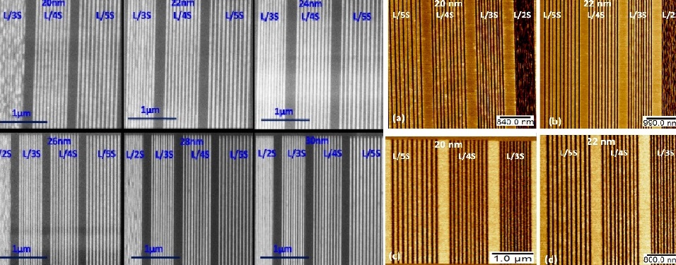
So far, the size of currently available chips has dropped to 22 nanometer node. The methods used currently include Deep Ultraviolet Lithography (DUVL). However, the DUVL has reached its potential and is unlikely to help in any further big development.
However, IIT Mandi is working on a next generation tool ‘Extreme Ultraviolet Lithography’ (EUVL). The research findings, so far, suggests good prospects for EUVL at 13.5 nm wavelength. This makes it feasible for mass production in near future. EUVL is cost-effective, offer higher unit throughput, and simplified working. Moreover, it could be extended to smaller sizes between 16nm to 10 nm. This brings EUVL at the centre of next generation IC fabrication and manufacturing.
Presently, the research team is facing some challenges that it needs to overcome before it could deliver the world with new era chips.
“However, current implementations of EUV lithography faces several challenges including that of finding photoresists that can concurrently achieve narrow line width around 16 nm, small line edge roughness at 3σ (1.5nm), and high photo sensitivity at 2-10mJ/cm2,” says IIT.
Prof. Kenneth and his team have achieved success in addressing the key problems causing the technical deficiencies in the current EUV photo resist technology. Prof. has already established the feasibility of developing a EUV photo resist with high sensitivity, high resolution, and low-line roughness.
The photo-resist materials in this case are directly sensitive to photons, while traditional technology requires chemical amplification.
Rs. 7 crore Funding for Research
So, IIT Mandi is at the verge of delivering next-gen photo-resists using EUVL. For its achievement in development of indigenous high end DUV, EBL and EUVL photoresists, IIT Mandi has procured funding of Rs. 7 crores from various Indian funding agencies including SCL (ISRO), DST and MHRD. Also, IIT Mandi is working on a bilateral resists technology program with the National Taiwan University (NTU).
Boost to Make in India
From the context of Make in India mission, this state-of-art technology would be helpful for Indian industries and entrepreneurs. IIT Mandi is at the forefront of Global competition on developing cutting-edge resists technology for sub-20 nm nodes. If the team delivers what it aims, it would be a giant leap for Indian semiconductor industries particularly Semiconductor Laboratory (SCL) , Mohali that are involved in 180 nm node technology. No Indian manufacturer develops these DUV resists, which is why SCL has to rely on foreign vendors. There is a dire need for indigenous technology to develop DUV resists.
IIT Mandi is also looking to organize an International conference on the “Trends in Technologies for Fabrication of Futuristic Semiconductor Devices – Make in India context” in early 2017. The idea is to gather international experts, scientists, technologists, industrialists and entrepreneurs to discuss and plan future strategies.
About the Research Team
An interdisciplinary team led by Prof. Kenneth Gonsalves, Visiting Distinguished Professor, IIT Mandi includes Dr. Subrata Ghosh (Organic Chemistry, Dr, Pradeep Parameswaran (Inorganic Chmistry), Both Associate Professors, School of Basic Sciences, Dr. Satinder Sharam (Electronic materials, Assistant Professor, School of Computing and Electric Engineering (SCEE) along with Postdoctoral research fellows Dr. Satyendra prakash Pal, Dr. pawan Kumar and Ph. D scholar guruprasad Reddy. In 2012, the team had started working the advanced Materials Research Centre (AMRC) of IIT Mandi.


